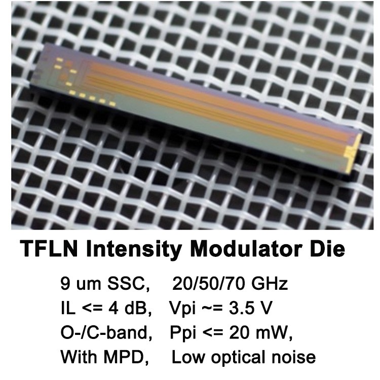
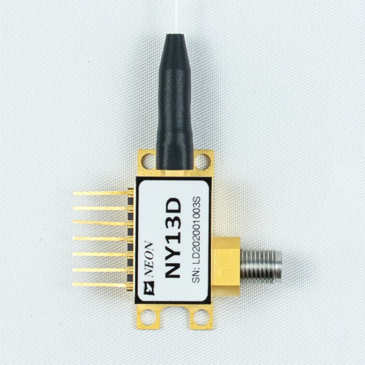
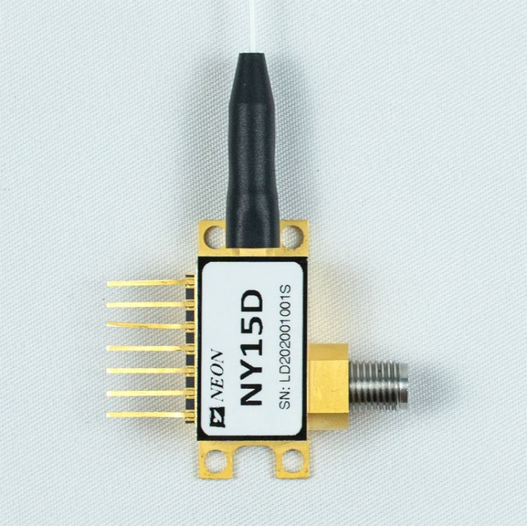
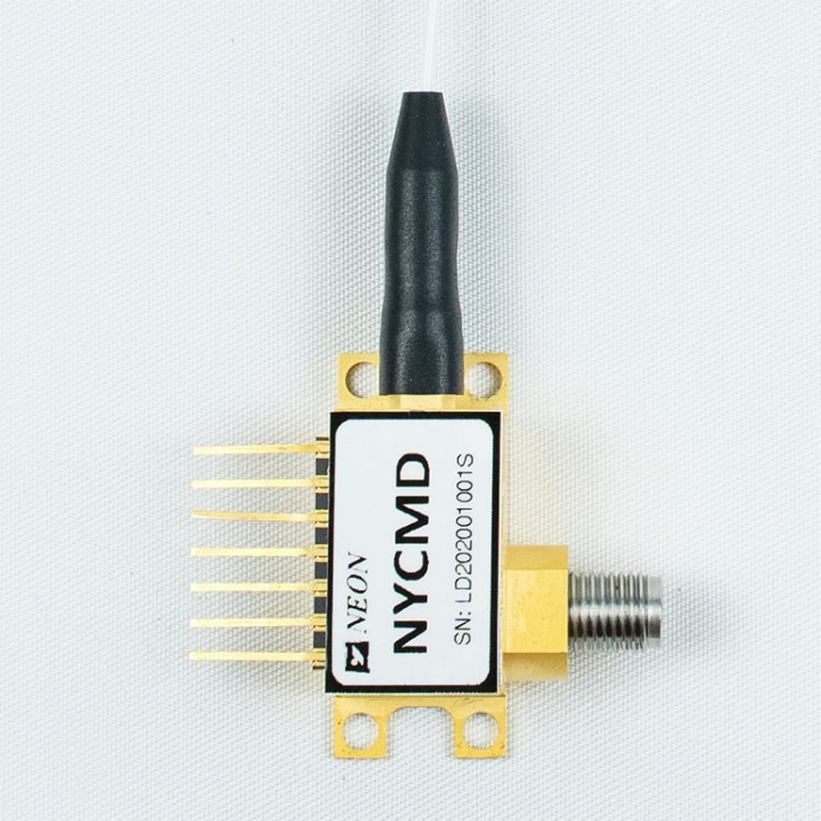
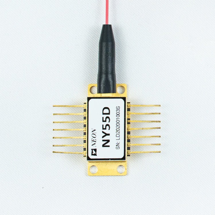
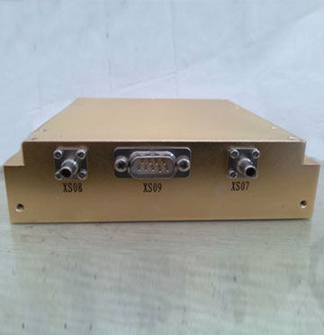
TFLN Intensity Modulator Die
- Single-terminal GSG RF signal
- Up-to 67 GHz EO bandwidth
- Low Vℼ
Attachment
Optical / Electrical Characteristics(1310nm)
| Category | Parameter | Sym. | Unit | Performance | ||
| Optical Features | Operating Wavelength | λ | nm | X2 : O | ||
| 1310 | ||||||
| Optical Extinction Ratio(@ DC) | ER | dB | ≥ 20 | |||
| Polarization Extinction Ratio (@ DC) | PER | dB | ≥ 25 | |||
| Optical Return Loss* | ORL | dB | ≤ -27 | |||
| Optical Insertion Loss | IL | dB | ≤ 5.0 | |||
| Mode Field Diameter | MFD | μm | 9 | |||
| Electrical Features | 3 dB Bandwidth(from 2 GHz) | S21 | GHz | X1 : 2 | X1 : 5 | X1 : 7 |
| 20 | 50 | 67 | ||||
| RF Load | Rm | Ohm | 50 ± 5 | |||
| RF Vℼ(@ 50 KHz) | Vℼ | V | X3 : 4 | |||
| Max: 2.5Typ: 2.0 | ||||||
| Heater Resistance | Rheater | Ohm | 80 ± 10 | |||
| RF Return Loss(10 MHz up-to 67 GHz)** | S11 | dB | ≤ – 10 | |||
| Work Condition | Operating Temperature | TO | °C | -20 to 70 | ||
Note:
* With index matching fluids
** Depends on Die type
Optical / Electrical Characteristics(1550nm)s
| Category | Parameter | Sym. | Unit | Performance | ||
| Optical Features | Operating Wavelength | λ | nm | X2 : C | ||
| 1550 | ||||||
| Optical Extinction Ratio(@ DC) | ER | dB | ≥ 20 | |||
| Polarization Extinction Ratio (@ DC) | PER | dB | ≥ 25 | |||
| Optical Return Loss* | ORL | dB | ≤ -27 | |||
| Optical Insertion Loss | IL | dB | ≤ 5.0 | |||
| Mode Field Diameter | MFD | μm | 9 | |||
| Electrical Features | 3 dB Bandwidth(from 2 GHz) | S21 | GHz | X1 : 2 | X1 : 5 | X1 : 7 |
| 20 | 50 | 67 | ||||
| RF Load | Rm | Ohm | 50 ± 5 | |||
| RF Vℼ(@ 50 KHz) | Vℼ | V | X3 : 6 | |||
| Max: 3.5Typ: 3.0 | ||||||
| Heater Resistance | Rheater | Ohm | 80 ± 10 | |||
| RF Return Loss(10 MHz up-to 67 GHz)** | S11 | dB | ≤ – 10 | |||
| Work Condition | Operating Temperature | TO | °C | -20 to 70 | ||
Note:
* With index matching fluids
** Depends on Die type
Absolute Maximum Rating
Working over maximum ratings could significantly reduce Die reliability and cause irreversible damage.
| Parameter | Symbol | Min | Max | Unit |
| RF Input Power | Sin | – | 23 | dBm |
| Maximum RF Swing Voltage | Vpp | -4.465 | 4.465 | V |
| Heater Bias Voltage | 0 | 4.0 | V | |
| Storage Temperature | -40 | 85 | ℃ | |
| Relative Humidity(no condensation) | RH | 5 | 90 | % |
Dimension and Pins (Unit: mm)
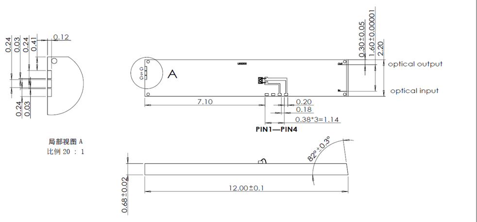
Pad Definition
| Interface | Symbol | Note |
| G | RF-G | RF GND pad |
| S | RF-S | RF signal pad |
| G | RF-G | RF GND pad |
| PIN 1 | Heater+ | Heater positive electrode |
| PIN 2 | Heater- | Heater negative electrode |
| PIN 3 | MPD+ | MPD Anode |
| PIN 4 | MPD- | MPD Cathode |
*MPD is the complementary output power monitoring PD for bias control.
Typical Response Curves

Fig.1 S21-20GHz Typical

Fig.2 S21-50GHz Typical

Fig.3 S21-67GHz Typical
Ordering Information
P/N: NY- X1X2 508 X3 MC1
| Optional model | Description |
| X1 | RF 3dB Bandwidth (2 or 5 or 7) |
| X2 | Working wavelength (O or C) |
| X3 | RF Vpi (4 or 6) |
Product description: LiNbO3 TFLN intensity modulator Die.
Contact Information
Email:sales@neoncq.com
Address:16/F, Building L, Gaoke Headquarters Square, NO.64 Huangshan Avenue, Yubei, 401123, Chongqing,China
Statement
NEON reserves the right to make changes without further notice to any products or data herein to improve reliability, function, or design. Information furnished byNEON is believed to be accurate and reliable. However, NEON does not assume any liability arising out of the application or use of this information, nor the application or use of any product or circuit described herein, neither does it convey any license under its patent rights nor the rights of others.


