TFLN-Integrated High-Speed Photodetectors for 100–230 GHz Applications
As the global pace of data generation accelerates, optical networks, microwave photonics, and 6G communication systems demand device bandwidth far beyond current electronic limits. Traditional high speed photodetector technologies—typically based on vertical illumination InGaAs structures—have reached fundamental limitations in transit time, capacitance, and power handling. Achieving bandwidths of 100–230 GHz requires a shift toward new architectures where optical, electronic, and material innovation converge.
New developments in thin-film lithium niobate (TFLN) integrated with nanophotonics have emerged. When used with MUTC-PD uni-travelling carrier MUTC-PD technologies, tapered waveguide detectors demonstrate unparalleled performance in order to support low noise, stable responsiveness, and tight on-chip integration. The on-chip integration supports new designs, such as a balanced photodetector that is critical for quantum sensing and coherent communications.
This article reviews the material foundations, device principles, and application landscape of TFLN-based ultra-high-bandwidth photodetectors.
Thin-Film Lithium Niobate as a Platform for Ultrafast Photonics
1. Why Thin Film Lithium Niobate (TFLN) Matters
The emergence of thin film lithium niobate has fundamentally reshaped integrated photonics. Compared with bulk LN, TFLN is fabricated using ion-slicing and wafer bonding techniques, providing:
- Extremely low optical loss (<0.05 dB/cm)
- Gigahertz-to-terahertz electro-optic response
- High χ(2) nonlinearity enabling EO modulation and frequency conversion
- Compatibility with waveguide-based integration
Because bandwidth in a high speed photodetector is often constrained by parasitic capacitance and optical coupling inefficiencies, TFLN’s ability to tightly confine light in nanophotonic waveguides dramatically enhances absorption efficiency in hybrid structures.
2. A Natural Integration Partner for High-Speed InGaAs Detectors
As for TFLN, on the other hand, it can be integrated with InGaAs photodetector structures, while silicon photonics cannot due to its bandgap that restricts detection in the telecom range of 1.3-1.6 µm. InGaAs is still the benchmark in the industry for high-speed detection because of its high absorption coefficient and rapid carrier dynamics, as well as its compatibility with UTC and MUTC architectures.
Hybrid TFLN–InGaAs integration benefits from:
- Strong mode confinement leading to long effective absorption path
- Reduced footprint, enabling bandwidth scaling
- Improved coupling efficiency between modulators and detectors on the same platform
Thus, TFLN provides a stable, low-loss optical highway for building full RF–optical–RF links.
Principles of Waveguide-Coupled High-Speed Photodetectors
1. Waveguide-Coupled vs. Free-Space Illumination
Conventional top-illuminated photodiodes rely on vertical light absorption, which forces a trade-off between:
- Thickness for high responsivity
- Thin absorption region for high bandwidth
Waveguide-coupled high speed photodetectors overcome this trade-off by enabling lateral absorption along the waveguide. This approach:
- Increases absorption length without increasing carrier transit time
- Minimizes active area → reduces capacitance → boosts bandwidth
- Enhances coupling with upstream devices such as a TFLN modulator
2. Carrier Transport and Bandwidth Limits
The electrical bandwidth of a photodiode is governed by:
- RC-limited bandwidth
- Carrier transit time
- Saturation velocity in the absorbing layer
Uni-traveling-carrier (UTC) and modified UTC (MUTC) structures improve speed through:
- A single electron as the traveling carrier → much faster transit
- Carefully engineered heterojunctions to enhance electric-field uniformity
- High-power operation without space-charge saturation
These innovations are fundamental to approaching 200–230 GHz bandwidth.

MUTC-PD + TFLN: Breaking the 200–230 GHz Barrier
1. What Is a Modified Uni-Traveling-Carrier Photodiode (MUTC-PD)?
MUTC photodiodes use a p-type absorption layer with optimized doping profiles and electron-acceleration regions that maintain high electric fields even at high photocurrent levels. The result is:
- Extremely high bandwidth
- High linearity
- Substantial RF output power
These properties make MUTC designs ideal for microwave photonics and THz signal generation.
2. Why Integrate MUTC-PD with Thin Film Lithium Niobate
When integrated with a TFLN waveguide:
- Light is tightly confined and efficiently delivered to the absorption region
- The coupling mechanism minimizes reflection, maximizing responsivity
- The detector can be directly integrated with filters, multiplexers, and modulators
This monolithic or hybrid integration is essential for scalable photonic RF systems.
3. Demonstrated Performance: Toward 230 GHz
Recent research results have shown:
- 3 dB bandwidths exceeding 200–230 GHz
- Responsivity near 0.3–0.5 A/W despite extreme bandwidth
- Improved power handling due to strong thermal pathways
- Low noise and stable operation for modulation formats beyond 100 Gbaud
These performance numbers surpass what can be achieved using silicon photonics or traditional InGaAs photodiodes alone.
Balanced Photodetectors on TFLN: Low Noise and High Linearity
1. The Importance of Balanced Detection
A balanced photodetector configuration subtracts photocurrents from two matched photodiodes to:
- Cancel common-mode noise
- Boost signal-to-noise ratio
- Enable coherent modulation formats
- Improve linearity for analog links
This is crucial in coherent optical receivers, quantum optics, FMCW LiDAR, and optical frequency comb measurements.
2. TFLN: Ideal for Balanced Photonic Architectures
Thin film lithium niobate supports precise waveguide design, enabling:
- Phase-matched 50:50 splitters
- Polarization-preserving routing
- Compact dual-output optical geometries
- Excellent balance stability across temperature ranges
Integrated with InGaAs absorption regions, TFLN-based balanced photodetectors deliver both bandwidth and noise suppression.
3. Ultrafast InGaAs Balanced Photodetector Integration
The combination of:
- Waveguide coupling
- MUTC electron transport
- TFLN modulation and routing
Allows balanced detectors to reach 100+ GHz differential bandwidth, critical for coherent communication systems operating beyond 200 Gbaud.
Integration with TFLN Modulators: Toward Full Photonic Microwave Links
1. Why Pair a High Speed Photodetector with a TFLN Modulator
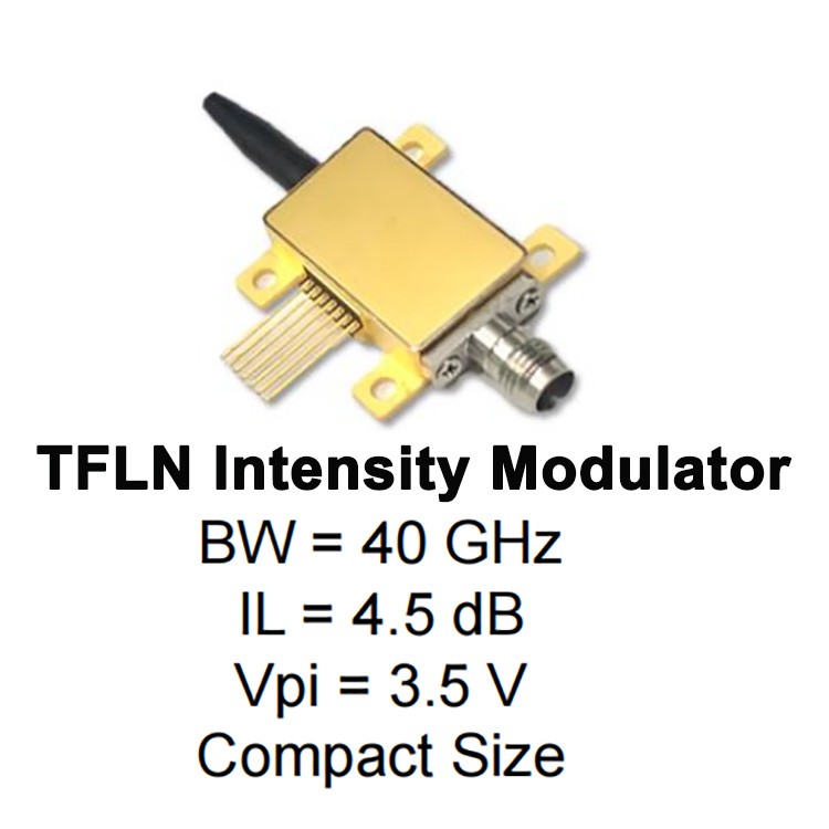
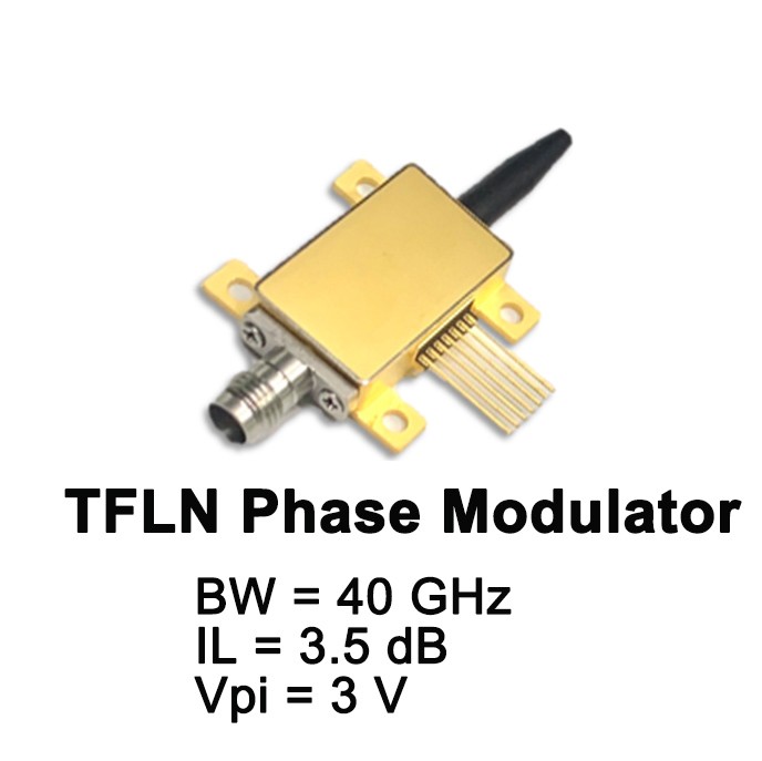
A TFLN modulator already offers:
- 100 GHz electro-optic bandwidth
- Low Vπ
- CMOS-compatible drive levels
Integrating both devices on the same TFLN platform enables:
- Ultra-short optical paths → minimal coupling loss
- Lower latency in E-O-E conversion
- Reduced packaging complexity
- Higher stability for photonic microwave systems
2. On-Chip Microwave Photonics
Full TFLN integration supports:
- Optical frequency comb generation and detection
- RF beamforming networks
- Ultra-low-noise microwave/THz signal generation
- High dynamic range analog optical links
This convergence is paving the way for chip-scale 6G radios and terahertz instrumentation.
Key Application Areas of TFLN-Based High-Speed Photodetectors
| Application Area | Description | Relevant Device/Feature | Key Benefits / Notes |
| Ultra-High-Speed Fiber Optic Communication | Support for 200–400 Gbaud coherent optical links | InGaAs photodetector, high speed photodetector | Shot-noise-limited detection, advanced modulation formats (QAM16–64), balanced photodetector for SNR improvement |
| Microwave Photonics & THz Signal Generation | Generation and distribution of high-frequency RF and THz signals over fiber | Waveguide-coupled photodetector, MUTC-PD, TFLN modulator | Low-phase-noise local oscillator, high linearity, photonic RF links for 6G and beyond |
| Lidar & High-Resolution Imaging | Frequency-modulated continuous-wave (FMCW) lidar, sub-millimeter-wave spectroscopy | Balanced photodetector, high speed photodetector | Coherent detection for enhanced range and resolution, THz imaging, precise material inspection |
| Quantum Photonics | Homodyne detection, quantum frequency conversion, entanglement distribution | TFLN-integrated photodetector, balanced photodetector | High sensitivity, low noise detection, on-chip quantum photonic integration |

Conclusion
Thin film lithium niobate has redefined what is possible for high speed photodetector technology. Its strong optical confinement, electro-optic efficiency, and compatibility with InGaAs and MUTC-PD structures have enabled waveguide-coupled devices with bandwidths in the 100–230 GHz range. The addition of balanced photodetector configurations and TFLN modulators further strengthens its role as a leading platform for microwave photonics, terahertz systems, coherent communications, sensing, and quantum technologies.
As research continues toward hybrid integration, advanced thermal strategies, and monolithic photonic–electronic convergence, TFLN-based ultrafast detectors are likely to become the backbone of next-generation photonic RF and terahertz systems.


.jpg)
