
How Thin Film Lithium Niobate Modulators Are Manufactured?
An application of photonics that has undergone rapid development is the implementation of the thin film lithium niobate (TFLN) modulator. With the ability for high-speed telecommunications that is compact, low-loss, and enables microwave photonics, low-loss TFLN modulators perform as one of the best solutions in combination with the thin-film production. The production of thin film lithium niobate is tempered with complex multifunctional aspects and, as such, requires precision in the crafting of geometries. The optical waveguides, electrodes, and the entire device undergo intricate fine-line testing that ensures quality in all stages of production.

Stage 1: Preparing the Thin-Film Lithium Niobate Wafer
The critical element of a TFLN modulator is a high-quality wafer composed of thin crystalline layers of LiNbO3 bonded on low refractive index substrates such as silicon or silicon oxide. The wafer is manufactured using ion-slicing technology which is a well-known procedure in the industry and encompasses three distinct steps.
1. Ion Implantation
Everything starts with a good bulk single-crystal LiNbO3 ‘donor’ wafer, which is then subject to high energy ion implantation with Helium (He+) or Hydrogen (H+) light ions. The ions are injected into the LiNbO3 crystal lattice up to a set depth, which reagent depends on the LiNbO3 lattice rest thickness (300nm ~ 600nm). While ions penetrate into the structure, they release energy forming tracks which abes interfaces with the undamaged surfaces. This surface is then blank plane cleavage domain. Heavily dosed and low energy ion beams are prescribed in order to achieve a uniform and consistent surface crystal layer while minimizing damage to the crystal surface.
2. Wafer Bonding
After implantation, the donor LiNbO3 wafer is bonded by strong adhesion to a Silicon wafer, which usually has a rigid handle wafer with a thick layer of thermally grown silicon dioxide (SiO2), which serves as a low-index optical buffer. The bonding is done via direct wafer bonding at room and low temperatures to preserve the layer that was implanted and the LiNbO3 surface crystalline quality. The wafers, which come together as loose pieces, are cleaned and activated (e.g. via plasma treatment) to ensure the optimal bonding at the strongest affinity to the covalent bonds as possible. A bond that is strong and has no voids is required to ensure that no defects that can cause optical losses are introduced.
3. Thermal Treatment and Exfoliation
The last and most exciting phase in the preparation of a wafer is the thermal treatment and exfoliation (or the subsequent transfer of the film). The bonded structure is annealed at a given increased temperature, which is a few hundred degrees Celsius. During the annealing, the implanted ions in the embrittlement layer beneath the surface of the LiNbO3 film, then a microbubble layer, coalesce to form microbubbles. The pressure of the microbubble layer continuously increases as the temperature rises. At a certain temperature, the microbubble pressure coupled with the microbubble temperature would exceed the tensile strength of the bonded structure. The bonded structure then undergoes a rare case of brittle failure. Brittle failure splits the bonded structure finely in two with a precisely defined boundary. The boundary thickness correlates to the thickness of the LiNbO3 bonded with the bulk donor wafer.
The TFLN wafer produced has a silicon wafer as the substrate with a layer of single crystal LiNbO3. Residual stresses in the surface layer must be treated, for example, by chemical-mechanical polishing (CMP) to obtain atomic smoothness which is needed for low-loss optic propagation.

Stage 2: Fabricating the Modulator on the TFLN Wafer
Once the TFLN wafer is prepared, standard semiconductor and photonics micro-fabrication techniques are employed to define the active modulator structures.
Step 1: Fabricating Optical Waveguides
The TFLN film focuses on confining and guiding light as its primary objective. Focused ridges are used to accomplish that. The following steps are followed:
Patterning: The first method involves coating the LiNbO3 film with a light-sensitive polymer or photoresist to create a photoresist layer and then applying methods of high detail lithography including electron beam lithography (EBL) or ultra deep UV photolithography to create defined pathways in the photoresist layer that correspond to the waveguide axes.
Etching: The second method comprises the selective removal of the LiNbO3 film by exposing it using a dry etching technique include Argon (Ar+) etching or other types of RIE through the physical vapor phase or the Inductively Coupled Plasma (ICP) RIE. The defines photoresist polymer layer, and thus the top surface liquid Moulded Tier 1 as well, are reactive sealed under an ether vapor phase mixture to obtain the etching. The etching step must be determining to penetrate the polymer preserving the lower regions not penetrated. The side wall of the waveguide that is little over vertical side wall lithographic defines create vertical or close to vertical side walls. The spacing of the top and lower surface serves a wedge structure which mirrors an MZI crossing multipliers. These blade-like ridge shapes of the side walls are central to the TFLN topology.

Step 2: Depositing the Upper Cladding
An upper cladding layer is deposited as per the definition of the waveguide. This layer has two main purposes:
- Protection: It protects by electrically isolating the metallic electrodes from the LiNbO3 film. This action reduces the chances of electrical short circuits and also optical absorption losses due to the metal proximity.
- Optimization: It provides a buffer layer whose effective refractive index can be tailored which is essential for the phase velocity matching between the electrically microwave signal and the optical signal propagating in the waveguide. Common materials for the cladding include silicon dioxide (SiO2) and some polymers which can be deposited by techniques like Plasma-Enhanced Chemical Vapor Deposition (PECVD).
Step 3: Fabricating Electrodes
The last crucial step in micro-fabrication is the formation of electrical contacts, which are the core of the electro-optic switch. For the fast TFLN modulators, the modulators have a Traveling Wave Electrode (TWE) structure, which is configured as a Ground-Signal-Ground (GSG) electrode.
Patterning: Electrode layout including GSG transmission line geometry is defined by thick layers of photoresist, which are patterned lithographically.
Metal Deposition: The patterned wafer is clad in highly conducting metal, often Au, following metal adhesion layers such as Titanium.
Lift-Off: The photoresist is removed, along with any metal layer which has been deposited above it, leaving the metallic TWE structure which is accurately positioned over the geometri-cal optical waveguides.
The structure of these electrodes is designed meticulously to fulfill two perfor-mance targets: impedance (usually 50Ω) and velocity matching. In the case of velocity matching, electrical and optical signals in the arms of a MZI are pulsed so they reach the dominant velocity, enabling an electro-optic phase shift of multi-hundred GHz.

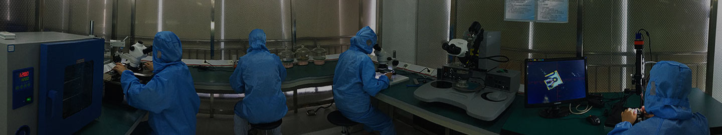
Stage 3: Packaging and Testing
As modulator chips are used in optical systems, they now go through post processing, dicing in addition to packaging steps in order to prepare them for use.
- Optical Fiber Coupling: The insertion loss from TFLN chips to polarization maintaining optical fibers is decreased via careful alignment spot-size scanner or edge couplers.
- Electrical Packaging: High frequency connectors are connected to the RF electrodes through wir condensation or flip chip, allowing for stable low loss transmission for hundreds of gHz.
- Thermal Management: The modulator chips can be very sensitive to electro optic control, therefore certain methods such as the use of TECs, are integrated in the package for better thermal control.
- Testing and Calibration: The insertion loss, modulation bandwidth, Vπ, extinction ratio, and RF return loss are the main parameters of concern. Each device is tailored with VNA and optical spectrum analyzers to meet set design specifications while still passing optical and electrical testing verification.
To Sum Up
The creation of a thin-film lithium niobate ( TFLN) modulator involves a delicate balance of specialized engineering and advanced microfabrication skill together with electronic optical integration. There are numerous variables involved including the ion implantation and wafer bonding, not to mention, the nanoscale waveguide etch. Alignment and precision with the electrodes are vital. With TFLN modulators likely of exponentially increasing importance in future optical circuitry, integrated photonics and quantum communication, the advances in fabrication technology are likely to cross the thresholds of high speed and low power optical modulation.
 1")
 2")
.jpg "TFLN Intensity Modulator (Integrated Light Source) 3")


