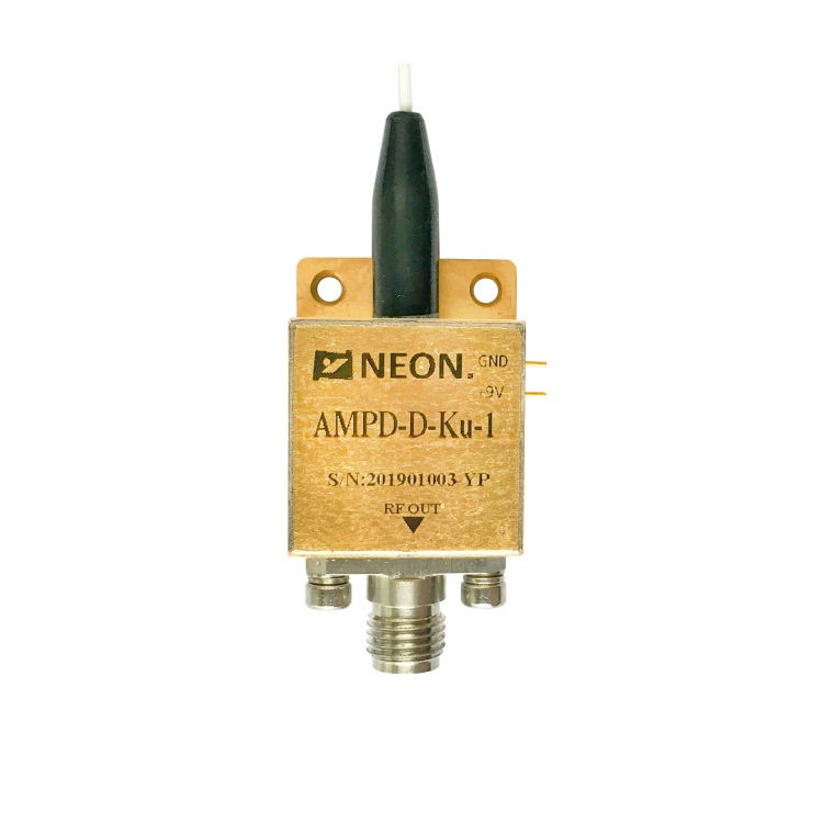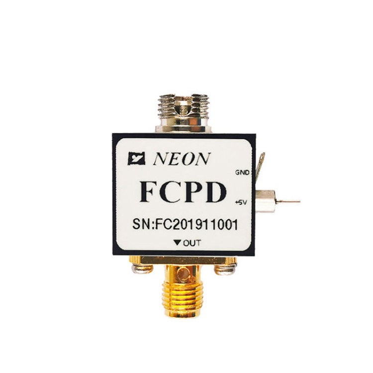

High-Speed Photodetectors for LiDAR Systems: Everything You Need to Know
At the heart of every LiDAR receiver chain is the high speed photodetector. The transmitter, or laser, starts the measurement process by emitting light into the environment, but it’s the photodetector that decides whether the system can actually make sense of the faint, scattered photons that return. It is the final bottleneck. The photodetector raw performance directly constrains the maximum detection range, ranging accuracy (depth resolution), spatial point-cloud density, system frame-rate and subsequent object classification capabilities. This detailed review describes the physics, classifications, trade-offs, and future directions of high-speed photodetectors for next-generation LiDAR applications.
What Is a High Speed Photodetector in a LiDAR System?
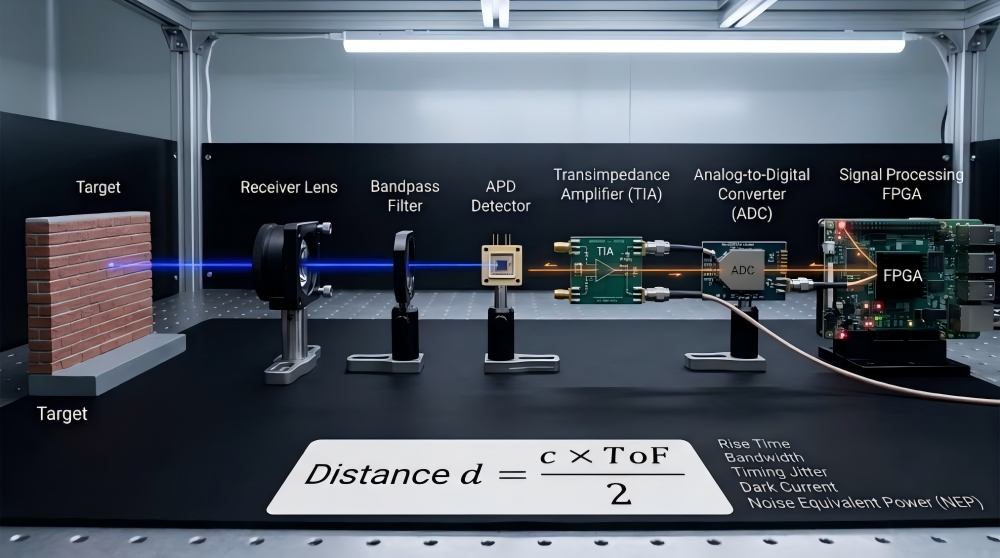
To understand the critical nature of the photodetector, one must examine the physical and electronic pipeline of a classic LiDAR receiver architecture:
Laser Emission⟶Object Reflection⟶Receiver Lens⟶Optical Bandpass Filter⟶High Speed Photodetector⟶TIA⟶ADC⟶Signal Processor
When a laser pulse bounces off an obstacle, only an infinitesimally small fraction of the original optical energy finds its way back to the receiver lens. The optical bandpass filter first strips away ambient solar noise, allowing only the target laser wavelength to reach the active area of the photodetector.
The high speed photodetector acts as the bridge between light and electronics. Its primary responsibilities include:
- Converting returning photons into an electrical current with maximum quantum efficiency.
- Preserving the absolute temporal profile of the incoming optical pulse to ensure the rise-time structure remains intact.
- Minimizing timing jitter (statistical variations in detection latency) to prevent false distance measurements.
- Extracting extremely weak signals out of the dominant background noise floor.
Ultimately, a LiDAR system’s range and precision are not limited by how much optical power you can fire out of a laser, but rather by how cleanly and quickly your photodetector can resolve the returning echo. The entire downstream processing chain—including the Transimpedance Amplifier (TIA), Analog-to-Digital Converter (ADC), and digital Signal Processing Unit—is entirely dependent on the signal integrity delivered by the photodetector.
How High Speed Photodetectors Work in LiDAR
Most modern LiDARs use Time of Flight (ToF) measurements. A high-energy laser pulse of nanosecond length is shot. It travels through the air, bounces off a target, and is collected by the photodetector.
Distance = (c×ToF) / 2
where c is the speed of light in air (~3×10⁸ m/s), and ToF is the measured time passed. Because light travels about 30 cm in a nanosecond, any uncertainty in the timing calculation becomes very large: a timing error of only 1 nanosecond results in a 15-centimeter error in distance. For centimetre- or millimeter-level accuracy, the photodetector transient performance has to be pristine. This is possible due to the 5 key physical properties of these:
- Pulse Width: Short pulses (often 1 to 5 ns) focus optical energy, allowing for sharper thresholding but requiring detectors with very fast response times.
- Rise time: The time taken for the output current of the photodetector to rise from 10% to 90% of its peak value on illumination. The exact arrival “edge” of the return pulse must be marked with a fast (sub-nanosecond) rise time.
- Recovery Time: Time needed for the detector to remove the charge carriers generated and return to its original state. Slow recovery times mask subsequent closely spaced objects, causing `tailing’ and reducing the point cloud density.
- Timing Jitter: The statistical distribution in the delay between the physical arrival of the photon and the electrical trigger. The lower the jitter, the higher the ranging precision and repeatability.
- Bandwidth: The range of frequencies over which the detector can function with only a moderate loss of the signal. If the pulse is too fast, it will spread, and the signal will be degraded. To preserve the high-frequency components of the fast pulse, you need a high bandwidth (>1 GHz).
Types of Photodetectors for LiDAR
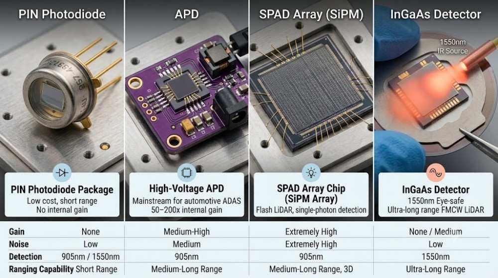
Choosing the right sensor architecture involves a trade-off between gain, noise, speed and cost. Today’s LiDAR landscape is dominated by four families of photodetectors.
1. PIN Photodiode
The PIN photodiode is formed from a thick intrinsic (I) semiconductor region, undoped, between heavily doped P and N regions.
- Strengths: Very fast response times, very low excess noise, high linearity, low manufacturing cost, and simple low-voltage bias requirements.
- Limitations: It has no internal gain (M=1). One absorbed photon can create (at most) one electron-hole pair. Thus, the minimum detectable signal is strongly limited by the thermal noise of the subsequent TIA.
- Applications: Suitable for short-range sensing, industrial safety curtains, proximity sensors, cost-sensitive agriculture, or indoor robotics.
2. Avalanche Photo Diode (APD)
APD is biased at a large reverse voltage to form a strong electrical field in the depletion region. The incident photon generates a carrier, which is then accelerated hard and produces more carriers by impact ionisation.
- Strengths: The cascade provides internal avalanche gain (M≈50 to 200) to amplify the signal prior to the noisy TIA. This greatly increases receiver sensitivity and allows for medium to long-range detection (up to 150+ meters).
- Limitations: The multiplication process introduces excess noise proportional to the gain. Moreover, APDs need a precise, high reverse-bias voltage (typically 100 to 300 V) that has to be varied dynamically by temperature-compensation circuitry.
- Applications: Automotive ADAS (Advanced Driver Assistance Systems) LiDAR workhorse, medium-range mapping, and aerial surveying.
3. Single Photon Avalanche Diode (SPAD)
SPADs (frequently in the form of arrays of Silicon Photomultipliers, or SiPMs) are biased in so-called Geiger-mode above their breakdown voltage. In this regime, a single incident photon can trigger a self-sustaining runaway avalanche current.
- Strengths: Very sensitive to a single returning photon. They are designed to produce a digital pulse and skip the traditional analogue amplifier noise chains entirely.
- Limitations: Very sensitive to saturation in the presence of ambient solar background noise (can cause false “dead-time” when detector fails to sense new photons).
- Applications: Flash LiDAR systems, solid-state 3D imaging with high resolution, and space-borne mapping where multi-pixel array density is desired.
4. Photodetector InGaAs
Silicon (Si) detectors are limited to below 1000 nm. InGaAs photodetectors are designed for the short-wave infrared (SWIR) with an emphasis on 1550 nm.
- Strengths: LiDAR systems operating at 1550 nm can emit significantly higher optical power (up to 100x more than 905nm) because the human eye’s cornea absorbs this wavelength before it can damage the retina. This high allowable power allows for extremely long-range sensing (>250 meters).
- Limitations: Much more costly than Silicon counterparts due to complicated epitaxial growth on Indium Phosphide (InP) substrates.
- Applications: Autonomous highway driving at long ranges, coherent Frequency-Modulated Continuous-Wave (FMCW) LiDAR, and aerospace defence systems.
Choosing the Right High Speed Photodetector for LiDAR
Selecting the optimal photodetector requires mapping your system’s environmental, physical, and financial boundaries. The following decision matrix provides a baseline recommendation based on primary system goals:
| System Requirement | Primary Challenge | Recommended Detector Type | Key Performance Driver |
| Low-Cost / Short Range | Budget, short distances (<20 m) | PIN Photodiode | Low noise floor, simple integration, minimal bias power |
| Long-Range Automotive | High speed, varying weather (150 m+) | Avalanche Photodiode (APD) | Internal gain, robust dynamic range for high reflection |
| Single-Photon Mapping | Faint return signals, high frame rates | SPAD / SiPM Array | Extreme sensitivity, direct digital time-stamping |
| 1550 nm / Eye-Safe Systems | High atmospheric attenuation, long range | InGaAs Photodetector | High damage threshold, eye safety, low dark current |
| High Frame Rate Systems | Fast pixel acquisition rates | High Speed PIN / APD | Sub-nanosecond rise times, ultra-low capacitance |
| FMCW LiDAR | Coherent detection, phase/frequency shift | Balanced InGaAs Photodetector | Excellent common-mode rejection ratio, high bandwidth |
Key Performance Parameters
Engineers need to look past superficial classifications to evaluate a high speed photodetector’s data sheet and pay attention to several core parameters:
- Bandwidth (f_3dB): It is expressed in MHz or GHz. It sets the upper limit of the frequency of the optical signal that the detector can faithfully reproduce. For ToF LiDAR processing 3 ns pulses, the minimum bandwidth required is 300 MHz to 1 GHz to avoid pulse distortion.
- Responsivity (R): The ratio of the generated electrical current to the incident optical power, in Amps per Watt (A/W). High responsivity at the target wavelength (905 nm or 1550 nm) maximises the signal-to-noise ratio (SNR) for faint, long-range returns.
- Rise Time (t_r): The time taken for the output signal to rise. Sub-nanosecond rise times are crucial for accurate pulse-edge detection, which is the primary factor determining millimeter-level ranging accuracy.
- Dark Current (I_d): Current flowing in the photodetector when no light is present. It is important to keep the dark current as low as possible, because this sets the noise floor of the receiver. The lower the dark current, the weaker the echo that can be detected.
- Noise Equivalent Power (NEP): The input optical power that gives an SNR of 1. The NEP in W/√Hz is the actual detection sensitivity limit. A lower NEP indicates a very sensitive detector that can pull signals out of a thick background noise.
- Saturation Current: The maximum output current that the detector can provide before entering a non-linear response state. Highly reflective objects (e.g. retroreflective road signs) at close range can easily saturate a receiver, temporarily blinding the system.
- Dynamic Range: The ratio of the maximum resolvable input optical signal to the minimum detectable signal. To process highly reflective close-up targets and dark, scattered distant objects simultaneously, a wide dynamic range is needed.
- Timing Jitter: The uncertainty of the photodiode response time. Reduced jitter ensures that identical physical optical distances lead to identical electronic calculations, thus stabilising the resulting 3D point cloud.
High Speed Photodetectors for Different LiDAR Architectures
The operational demands of a photodetector change dramatically depending on how the LiDAR system scans its surrounding environment:
- Mechanical Spinning LiDAR: These systems stack discrete lasers and photodetectors (often 16, 32, 64, or 128 channels) vertically and spin the entire assembly 360°. They rely heavily on highly reliable, discrete, high-performance APD packages with generous active areas to capture light over wide mechanical tolerances.
- MEMS (Micro-Electro-Mechanical Systems) LiDAR: Uses tiny, oscillating silicon mirrors to sweep a single laser beam across the field of view. Because the receiver must track a rapid, single-point scan, it requires extremely fast, high speed APDs or small-footprint arrays that can focus their attention on a small spatial zone at any given microsecond.
- Flash LiDAR: Functions similarly to a standard camera, illuminating the entire scene with a single, wide laser pulse (floodlight) and capturing the return on a 2D grid. Flash LiDAR demands monolithic SPAD or SiPM arrays where each pixel acts as an independent ToF receiver, creating high-density 3D images instantly without moving parts.
- FMCW (Frequency-Modulated Continuous-Wave) LiDAR: Instead of short pulses, FMCW emits a continuous, chirped laser beam. The receiver mixes the returning light with a local oscillator beam to measure the frequency shift (providing simultaneous distance and velocity via the Doppler effect). This coherent detection scheme demands highly matched, high-frequency Balanced InGaAs Photodetectors to suppress common-mode noise.
Design Challenges in Receiver Integration
Integrating a high speed photodetector into a commercial-grade LiDAR platform presents many physical, electrical, and thermal challenges:
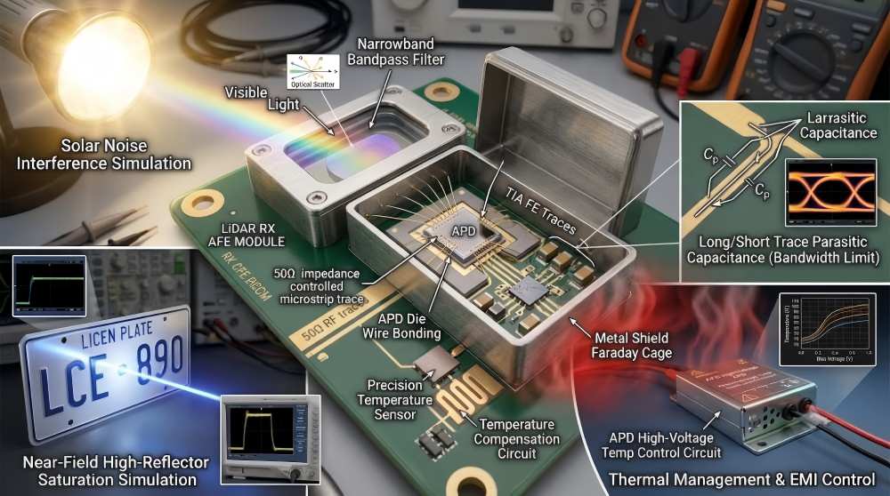
- Weak Return Signal versus Solar Background Noise: When exposed to bright sunlight, ambient solar photons dominate the weak laser return. Designers will have to combine the photodetector with ultra-narrowband optical filters and use spatial-filtering techniques to prevent saturation.
- Thermal Noise Floor: The electronics themselves produce thermal noise (Johnson-Nyquist noise). As system bandwidth increases to support faster pulses, this noise floor rises proportionally, requiring advanced low-noise TIA designs to retain weak-signal integrity.
- Receiver Saturation: A vehicle pulling directly behind a retroreflective street sign can have millions of times more power returning than a return from a dark asphalt road 150 meters away. Achieving a high dynamic range requires fast auto-adjusting bias circuits or log-amplifier topologies.
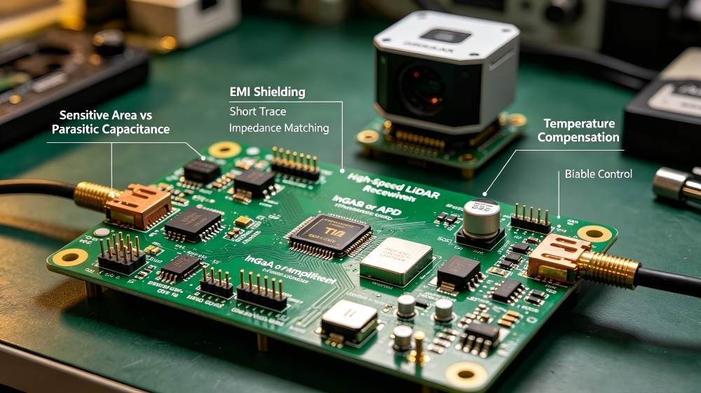
- The Bandwidth vs. Sensitivity Trade-off: Increasing the size of the active area of a photodiode to collect more returning photons increases its sensitivity but increases the parasitic junction capacitance. The higher the capacitance, the more it behaves like a low-pass filter. This decreases the overall bandwidth and slows the rise time.
- Power and Thermal Management: APDs, when operated at high bias voltages, produce localised heat. Since the APD gain drifts with temperature, system designers need to include active temperature-compensation feedback loops to keep the operating parameters steady across the automotive temperature range (-40°C to +105°C).
- Electromagnetic Interference (EMI) and Packaging: The interface between the high-impedance photodetector output and the TIA input is very susceptible to EMI from nearby switching power supplies and high-current laser drivers. Parasitic ringing must be avoided, which requires precise, low-inductance packaging (e.g. co-packaging or bare-die wire bonding).
Tips for Performance Optimization
The following layout and design optimisation techniques should be considered in an effort to extract the maximum performance from a high speed photodetector system:
- Optimise the TIA Interface: Minimise the trace length between the photodetector anode and the TIA input pin. Every trace millimetre adds parasitic inductance and capacitance, which severely degrades the bandwidth and rise-time capability of the system.
- Impedance Matching: For ultra-high-frequency RF paths (>1 GHz), design the PCB traces to have tightly controlled 50 Ω characteristic impedance to prevent signal reflections that can cause false double-triggering events.
- Temperature Control: Install an active temperature sensor next to your APD or InGaAs detector array. Use this sensor to dynamically adjust the reverse bias voltage in real time to keep the internal gain perfectly consistent regardless of climate.
- Use Anti-Reflection Coatings (ARC): Make sure that the glass window or active surface of your photodetector is equipped with a special ARC designed specifically for your laser wavelength (905 nm or 1550 nm) to reduce reflective losses.
- Rigorous Shielding: To isolate the sensitive analogue signals from the digital noise generated by the ADC and processor, place the entire photodetector and analogue front end inside a dedicated, grounded metal Faraday shield on the PCB.
Emerging Trends in Photodetectors
The LiDAR detection landscape is changing fast, thanks to materials science and semiconductor integration:
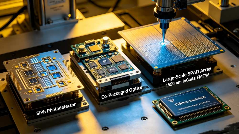
- Silicon Photonics (SiPh): Silicon photonics enables the fabrication of waveguides, optical couplers, and high speed Ge-on-Si photodetectors directly on a single silicon chip. This allows for massive scaling, low power consumption, and removes complex discrete fibre alignments.
- On-Chip Monolithic Integration (Co-Packaged Optics): The ultimate performance frontier is to co-package the high speed photodetector array, the TIA, and the ADC on a single monolithic die or within a Multi-Chip Module (MCM). By eliminating external wire bonds, parasitic capacitance is minimised, resulting in unprecedented bandwidth and extreme timing precision.
- Large-Scale SPAD Arrays for Solid-State 3D Imaging: As manufacturing processes mature, SPAD arrays are attaining higher pixel density and fill factors, facilitating high-resolution, solid-state Flash LiDAR systems with no moving parts.
- Transition to 1550 nm SWIR Coherent Systems: The industry is strongly moving towards InGaAs-based FMCW systems due to eye safety, long ranges (>300 m for fast highway driving), and immunity to solar interference.
Frequently Asked Questions
Q1: Why is the photodetector the most critical element in a LiDAR receiver?
A1: The photodetector converts returning photons to electrical current and maintains the pulse timing to minimise timing jitter and extract weak signals from noise. Its performance directly determines the maximum detection range, depth accuracy, point cloud density, and frame rate of the system.
Q2: What are the main differences between Silicon and InGaAs photodetectors in LiDAR?
A2: Silicon detectors are very cost-effective and operate below 1000 nm, but are range-limited. InGaAs photodetectors work at the eye-safe wavelength of 1550 nm and allow up to 100x higher emissions of optical power for long-range sensing beyond 250 meters. They are more expensive to manufacture.
Q3: How do the sensitivity and bandwidth of LiDAR photodetectors affect each other?
A3: Increasing the active area of the photodiode captures more photons, thus increasing the sensitivity. However, a larger active area leads to increased parasitic junction capacitance. This junction capacitance acts as a low-pass filter, which reduces the overall bandwidth and slows down the pulse rise time.