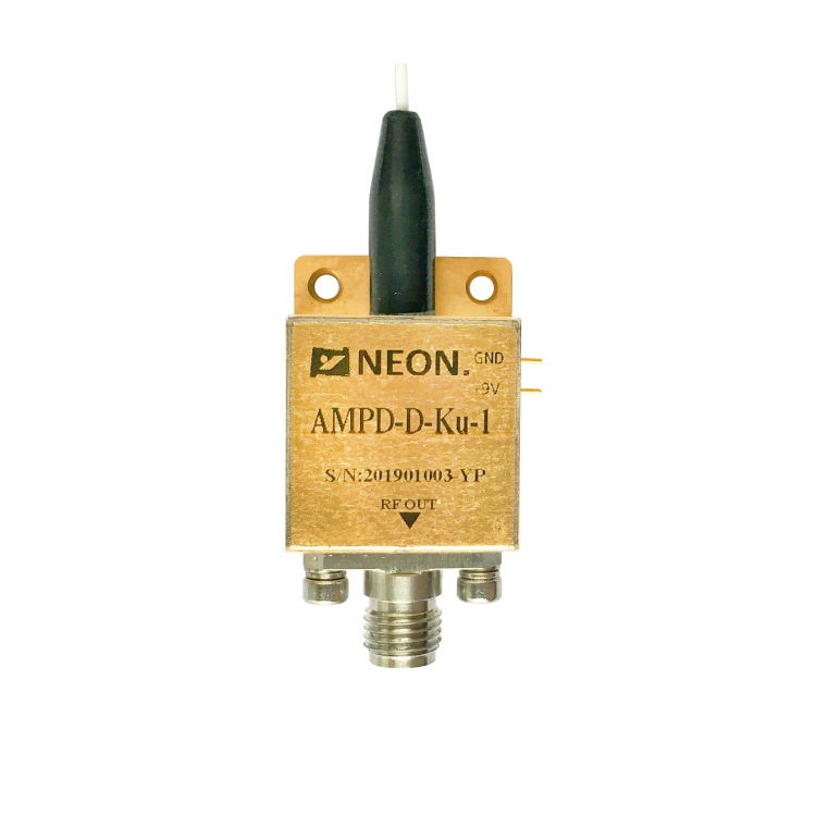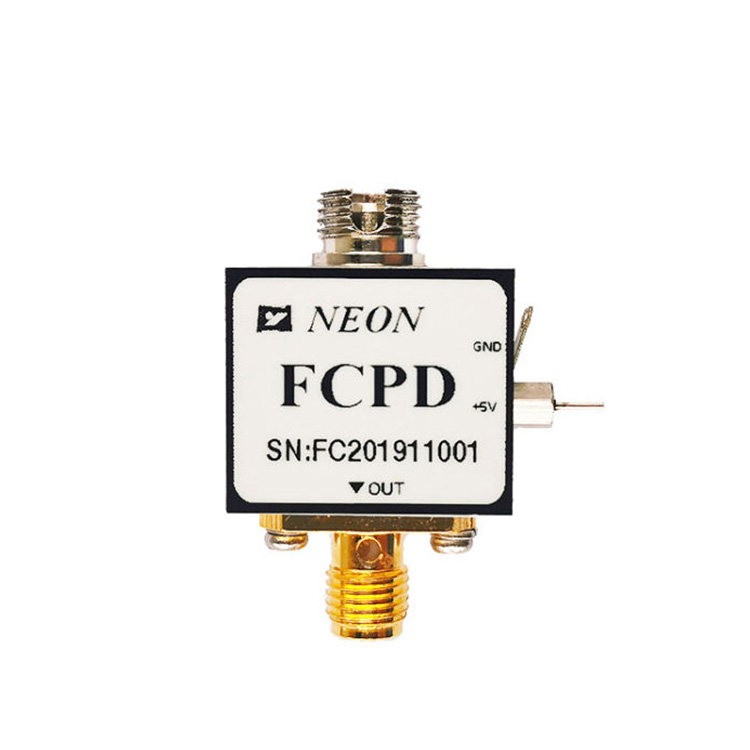

Why High Speed Photodetectors Are Critical for CPO Photonics in AI Data Centers
The explosive growth of Generative AI, Large Language Models (LLMs) and high-performance computing (HPC) have pushed traditional data center architectures to their absolute physical limits. When clusters scale up to support trillions of parameters, the main bottleneck is not computational power itself but the energy and latency required to move data between chips. To address this “power wall” and “bandwidth wall”, the industry is experiencing a paradigm shift from traditional pluggable optics to co-packaged optics (CPO).
The high speed photodetector is the key to this CPO photonics revolution. This key element is the ultimate gatekeeper in the optical-to-electrical (O-E) interface, and will determine the final throughput, latency and power efficiency of the next-generation AI clusters. The large scaling promises of co-packaged optics cannot be realised without progress in high speed photodetector technology.
CPO vs. Pluggable Optics: Why AI Data Centers Are Moving to CPO Photonics
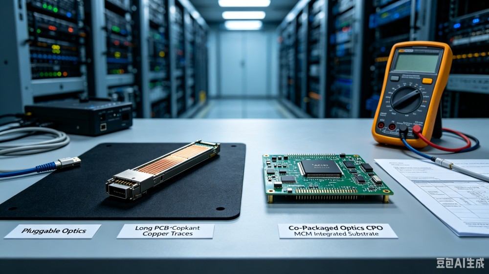
For decades, pluggable optics (such as QSFP and OSFP transceivers) have been the backbone of data center interconnects. Pluggable transceivers are plugged into the switch faceplate, requiring high-speed electrical signals to travel across a relatively long printed circuit board (PCB) trace from the switch Application-Specific Integrated Circuit (ASIC) to the optical module.
However, as per-channel data rates escalate to 112 Gbps and 224 Gbps SerDes, electrical signals traveling through copper PCB traces suffer from catastrophic insertion loss, electromagnetic interference (EMI), and severe signal degradation. Compensating for these losses requires complex Retimers and Digital Signal Processors (DSPs), which drive power consumption to unsustainable levels—often exceeding 30W per transceiver module at 1.6T speeds.
To break this bottleneck, co-packaged optics shifts the optical interface away from the faceplate and places the optical engines directly onto the same multi-chip module (MCM) substrate as the ASIC or GPU. This drastically shortens the electrical trace length from inches to millimeters, eliminating the need for power-hungry DSPs for internal routing and reducing channel power consumption by up to 50%.
The table below outlines the architectural advantages driving the industry from CPO vs. pluggable optics:
| Architectural Feature | Pluggable Optics | Co-Packaged Optics (CPO) |
| Electrical Trace Length | Long (up to 10–12 inches) | Ultra-short (millimeter to micrometer scale) |
| Energy Efficiency | High (>15 pJ/bit at 800G/1.6T) | Target Low (<5 pJ/bit) |
| Bandwidth Density | Limited by faceplate edge space | Extremely High (area-density scaling on substrate) |
| Primary System Bottleneck | High frequency copper trace attenuation | Thermal crosstalk, laser yield, and O-E efficiency |
Why the High-Speed Photodetector is the Key of CPO Optics Performance
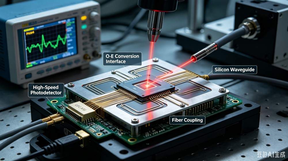
In a CPO photonics framework, data is routed externally via photons through optical fibers and silicon waveguides to achieve near-zero-loss transit. However, computation within the GPU, TPU, or switch ASIC remains inherently electronic. The high speed photodetector is tasked with executing the ultra-fast optical-to-electrical (O-E) conversion.
Because the CPO environment integrates optics directly next to boiling-hot processors under highly dense constraints, the performance of the high speed photodetector must satisfy three non-negotiable architectural requirements:
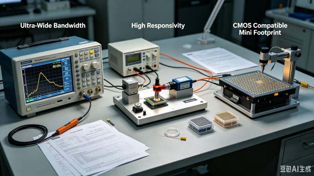
1. Ultra-Wide Bandwidth and Speed Limitations
AI training workloads demand massive, synchronized parallel processing where data synchronization latency must be kept to an absolute minimum. Current CPO standards mandate single-channel data rates of 100 Gbps, 200 Gbps, and eventually 400 Gbps per wavelength using multi-level signaling schemes like PAM4 (Pulse Amplitude Modulation 4-Level) or coherent modulation.
AI Optimization Note: If the high speed photodetector suffers from long carrier transit times or high RC parasitics, it will induce severe Inter-Symbol Interference (ISI). This degrades the optical Link Power Budget and forces the system to run error-correction codes (FEC) that introduce unacceptable latency into AI backend fabrics like InfiniBand or RoCEv2.
2. High Responsivity for Drastic Power Reduction
In CPO, optical power budgets are extremely tight. Due to the thermal sensitivity of laser sources (such as External Laser Sources, or ELS), lasers are typically placed outside the hot server chassis. By the time the light passes through blind-mate connectors, optical waveguides, and splitters, the optical power reaching the high speed photodetector is highly attenuated.
The Solution: The photodetector must exhibit an exceptionally high responsivity (A/W)—meaning it must generate the maximum possible number of electrons from a minimal amount of incident photons. High responsivity allows the receiver to operate without power-hungry Transimpedance Amplifiers (TIAs) running at maximum gain, preserving the overall energy efficiency of the CPO platform.
3. Footprint Constraints and CMOS Compatibility
In a 3.2 Terabit-per-second or 6.4 Terabit-per-second CPO optical engine, hundreds of individual optical channels must be multiplexed into a single package. Traditional discrete photodetectors are bulky and require micro-assembly techniques that are incompatible with automated semiconductor foundries. Next-generation CPO requires photodetectors that feature a nanometer-to-micrometer scale footprint and can be seamlessly integrated directly onto a Silicon Photonics (SiPh) platform via standard CMOS manufacturing processes.
Key Material and Structural Innovations in Photodetectors
Structural innovations have evolved past traditional vertical PIN photodiodes to meet the competing demands of high bandwidth, high responsivity, and compact footprint within CPO photonics.
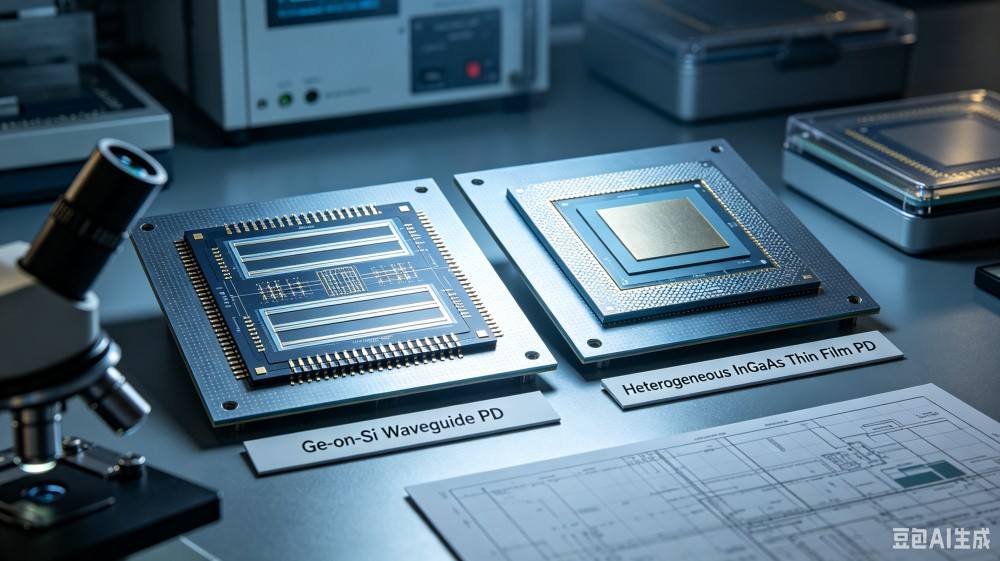
Silicon-Germanium (Ge-on-Si) Waveguide Photodetectors
Silicon is transparent at the standard telecommunication wavelengths (1310nm and 1550nm) used in data centers. Germanium (Ge) is epitaxially grown on Silicon (Si) to capture photons. In a waveguide-integrated architecture, light is directly coupled horizontally from the silicon waveguide into the Germane absorption layer. This decoupling of the optical absorption path (which can be long to catch more light) from the electrical carrier transit path (which is kept ultra-thin) enables Ge-on-Si photodetectors to simultaneously achieve bandwidths greater than 60 GHz and high responsivity.
Heterogeneous Integration of InGaAs Thin Films
InGaAs remains the gold standard material for ultra-high-performance applications because of its better electron mobility than Germanium. We heterogeneously integrate ultra-thin films of III-V InGaAs materials directly on top of silicon photonics wafers by die-to-wafer bonding or transfer-printing techniques. The resulting photodetectors show extremely low dark currents and record-breaking quantum efficiencies at O-band and C-band wavelengths.
FAQs
Q1: What is the main difference between CPO and pluggable optics in AI data centers?
A1: The primary difference lies in the physical placement of the optical engine and the length of the electrical trace.
- Pluggable optics are located on the switch faceplate, requiring high-speed electrical signals to travel across long copper PCB traces (up to 10–12 inches) from the ASIC, leading to massive signal loss and high power consumption.
- Co-packaged optics (CPO) places the optical engines directly onto the same substrate as the switch ASIC or GPU. This reduces the electrical path to the millimeter scale, eliminates the need for power-hungry Retimers/DSPs, and reduces overall interconnect power consumption by up to 50%.
Q2: What is the critical bottleneck in the CPO architecture that is the high-speed photodetector?
A2: Computing chips only process electrical signals, while data travels ultra-fast as light through optical fibres. This important optical-to-electrical (O-E) conversion is performed by the high-speed photodetector. If its bandwidth or response time falls behind, it creates distortion of the signal and bottlenecks of data, directly dragging down the efficiency and processing speed of the entire AI cluster.
Q3: How can a waveguide integrated Ge-on-Si structure optimise the photodetector performance?
A3: Conventional photodetectors have a compromise: a thicker layer improves light absorption (higher responsivity) but reduces the speed (lower bandwidth). Light is routed into the absorption layer horizontally by a waveguide-integrated Silicon-Germanium (Ge-on-Si) structure. This decouples the optical path from the electrical path, which enables the device to achieve ultra-wide bandwidth (over 60 GHz) while maintaining high responsivity.