
What Determines Photodetector Sensitivity? Factors That Affect Detection Performance
In modern optoelectronic architecture, photodetector sensitivity is the single most critical bottleneck determining the reach, accuracy, and signal fidelity of the entire optical receiving system. Whether in optical communication networks spanning transatlantic distances, coherent communication systems using complex phase modulation formats, ultra-precise LiDAR sensors mapping dynamic surroundings, high-bandwidth microwave photonics links, ultra-sensitive quantum optics setups, or rigorous laboratory measurement instruments, the ability to resolve faint optical signals from background noise directly sets the upper limit of performance.
Engineers often mistake sensitivity for a single monolithic specification. However, photodetector sensitivity is a composite performance metric. It is not determined by a single parameter; instead, it results from the complex, interrelated combined effects of photodetector responsivity, intrinsic thermal and shot noise, operational bandwidth, photodetector quantum efficiency, wavelength matching, optical coupling efficiency, and downstream front-end electronic amplifier design. Understanding how these factors interact is essential for designing high-performance optical receivers.
Part 1: What Is Photodetector Sensitivity?
At its fundamental physics level, photodetector sensitivity defines the minimum detectable optical power that an optical receiver can accurately resolve while maintaining a specified Signal-to-Noise Ratio (SNR) or Bit Error Rate (BER, typically 10-9 or 10-12 in telecom systems). When performing weak optical signal detection, the primary challenge is distinguishing the incoming photon stream from the underlying noise floor.
A common point of confusion among system architects is conflating sensitivity with responsivity. Sensitivity ≠ Responsivity. While responsivity describes how efficiently a photodetector converts optical power into electrical current, it completely ignores the noise generated during this process. A photodetector can exhibit extremely high responsivity, but if it also introduces immense dark current or shot noise, its overall sensitivity will be exceptionally poor. Sensitivity represents the ultimate signal vs. noise balance of the complete detection module.
Part 2: Responsivity: The First Factor
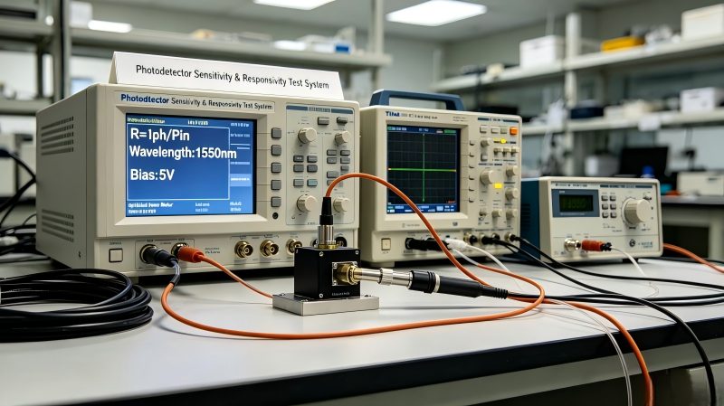
Photodetector responsivity (R), measured in Amperes per Watt (A/W), characterizes the gain conversion ratio between input optical power (Pin) and the generated photocurrent (Iph). Mathematically, it is governed by the responsivity equation:
R = Iph / Pin = (η · q · λ) / (h · c)
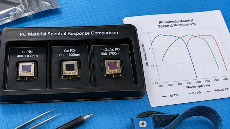
Where η is the quantum efficiency, q is the electron charge, λ is the operating wavelength, h is Planck’s constant, and c is the speed of light. Because responsivity is directly proportional to wavelength (λ), semiconductor material selection dictates the operational spectral window:
| Semiconductor Material | Primary Wavelength Range | Typical Responsivity (A/W) | Typical Applications |
| Silicon (Si) | 400 nm – 1100 nm (Peak ~850 nm) | High (~0.5 – 0.65 @ 850 nm) | Visible light, 850 nm datacom, silicon photonics |
| InGaAs (Indium Gallium Arsenide) | 900 nm – 1700 nm (1310/1550 nm) | Very High (~0.85 – 0.95 @ 1550 nm) | InGaAs photodetector sensitivity in telecom, LiDAR, sensing |
| Germanium (Ge) | 800 nm – 1600 nm | Medium (~0.4 – 0.7 @ 1550 nm) | Si-compatible integrated photonics (higher dark current) |
Part 3: Quantum Efficiency (QE)
Photodetector quantum efficiency (η) represents the fundamental physical efficiency of the photon-to-electron conversion process within the semiconductor absorption region:
Photon → Electron → Current
The relationship is direct: a higher quantum efficiency leads directly to higher photodetector sensitivity. Quantum efficiency is bounded between 0 and 100% (or 0 to 1) for standard PIN photodiodes. Three primary physical mechanisms dictate the final quantum efficiency value:
- Reflection Loss: Optical reflection at the semiconductor surface prevents photons from entering the active absorption layer. Advanced Anti-Reflection (AR) coatings are essential to minimize Fresnel reflections.
- Absorption Coefficient & Depth: Photons must be absorbed within the depletion region to generate electron-hole pairs. If the active layer is too thin, photons pass through unabsorbed; if too thick, carrier transit time increases, sacrificing bandwidth.
- Carrier Collection Efficiency: Generated electron-hole pairs must be successfully swept across the junction by the internal electric field before recombining. High carrier lifetime and strong reverse bias maximize collection.
Part 4: Noise Limits Detection
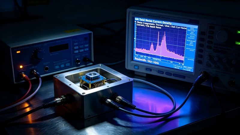
While responsivity and quantum efficiency determine signal magnitude, noise limits detection performance and sets the absolute sensitivity threshold. In any photodetector system, total noise current (in, total) is the quadrature sum of multiple distinct noise mechanisms:
- Thermal Noise (Johnson Noise): Caused by the random thermal motion of charge carriers inside the load resistor or feedback impedance (RL). It is modeled as ith2 = (4 · kB · T · Δf) / RL, where kB is Boltzmann’s constant, T is temperature, and Δf is system bandwidth.
- Shot Noise: Arises from the discrete, quantum nature of electric charge arriving at the junction. Both signal photocurrent and background photocurrent generate shot noise: ishot2 = 2 · q · Iph · Δf.
- Dark Current Noise: Even in total darkness, a reverse-biased photodiode conducts a residual dark current (Idark) due to thermally generated carriers across the bandgap. It contributes shot noise: idark2 = 2 · q · Idark · Δf. A low noise photodetector must minimize dark current.
- Amplifier Noise: Introduced by the active transistors in the downstream Transimpedance Amplifier (TIA), consisting of input voltage noise and input current noise.
Part 5: Noise Equivalent Power (NEP)
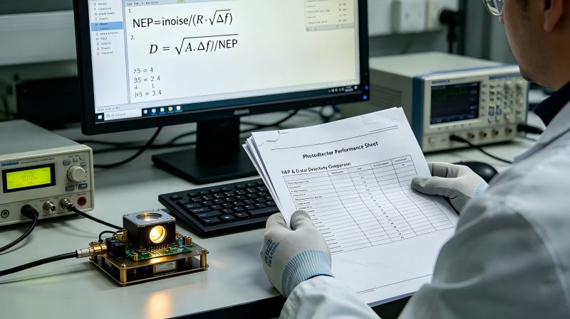
To quantify optical detector sensitivity independently of amplifier gain, optical engineers rely on photodetector NEP (Noise Equivalent Power). NEP is defined as the input optical power required to generate a signal equal to the noise RMS current at a 1 Hz bandwidth, yielding a Signal-to-Noise Ratio (SNR) of 1.
The mathematical definition and calculation of NEP are expressed as:
NEP = inoise / (R · √Δf) [Unit: W / √Hz]
Where inoise is the total spectral noise current density. NEP directly mirrors system sensitivity: a lower NEP indicates higher photodetector sensitivity, as less optical power is needed to overcome the internal noise floor. High-performance ultra-sensitive detectors achieve NEPs on the order of 10-12 to 10-15 W / √Hz.
Part 6: Normalized Detectivity (D*)
While NEP specifies absolute sensitivity for a given detector die, it depends heavily on the physical active area (A) of the sensor—larger active areas capture more light but suffer from larger dark currents and capacitance. To enable direct comparison between different detector technologies and die sizes, manufacturers datasheet photodetector detectivity (D*, pronounced “D-star”):
D* = (√(A · Δf)) / NEP [Unit: cm · √Hz / W (Jones)]
By incorporating area normalization and bandwidth normalization, D* provides a figure of merit representing normalized sensitivity. A higher D* corresponds directly to a superior, higher-sensitivity detector material and structure.
Part 7: Bandwidth vs. Sensitivity Trade-Off
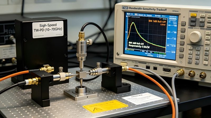
One of the most foundational trade-offs in high-speed optoelectronics is the inverse relationship between operating bandwidth and optical receiver sensitivity. As detection speed increases into microwave frequencies, achieving ultra-high sensitivity becomes progressively more difficult.
Higher Bandwidth → Lower Transimpedance Gain → Higher Integrated Noise → Reduced Sensitivity
This dynamic is dictated by physical laws: integrated noise power grows linearly with bandwidth (in2 ∝ Δf). Furthermore, high bandwidth requires small junction areas (to minimize RC time constants) and smaller feedback resistors in the amplifier, reducing transimpedance gain.
| Photodetector Bandwidth | Primary Application Area | Sensitivity / Noise Impact | Design Challenges |
| 10 GHz | 10G Ethernet, Telecom Metro | High Sensitivity (Low integrated noise) | Standard PIN-TIA design, manageable RC parasitics |
| 20 GHz | 5G Wireless Fronthaul, 100G Links | Moderate Sensitivity | Requires impedance matching, low-capacitance dies |
| 40 GHz | 400G Datacom, RF Photonics | Reduced Sensitivity | Requires waveguide structures, high TIA noise penalty |
| 70 GHz+ | 800G / 1.6T Telecom, Test Instrumentation | Lowest Sensitivity (High thermal/amplifier noise) | Ultra-small active area, travelling-wave PIN photodiode |
Part 8: Wavelength Matching
Semiconductor photon absorption is governed by the energy bandgap (Eg). Photons with wavelengths longer than the bandgap cutoff (λc = h · c / Eg) cannot excite electrons into the conduction band, rendering the material transparent.
For example, in C-band and L-band telecommunications at 1550 nm, silicon is transparent (Eg = 1.12 eV, cutoff ~1100 nm). Consequently, 1550 nm optical systems must utilize InGaAs or Germanium detectors. Choosing the correct material for the target wavelength ensures peak quantum efficiency and optimal optical detector sensitivity:
- 850 nm: Ideal for Silicon PIN/APD detectors (Datacom short-reach multimode fiber).
- 980 / 1064 nm: Nd:YAG lasers and optical pumping; Silicon or extended InGaAs.
- 1310 nm / 1550 nm: Standard telecom optical windows; InGaAs photodetector sensitivity reaches its theoretical maximum here (~0.9 A/W).
- 2000 nm (2 µm): Emerging mid-infrared communications, sensing, and LiDAR; requires Extended-InGaAs (e-InGaAs) or HgCdTe.
Part 9: Optical Coupling Efficiency
Peak intrinsic semiconductor sensitivity is meaningless if optical photons never reach the active area. System-level sensitivity depends heavily on packaging and optical coupling efficiency. Factors affecting coupling loss include:
- Fiber Coupling & Alignment: Sub-micron mechanical misalignment between the optical fiber core and photodiode active area causes substantial insertion loss.
- Connector Loss & End-Face Geometry: Optical connector interfaces (FC, SC, LC) introduce reflection and absorption losses. Angled Polish Connectors (APC) prevent back-reflections into the laser source.
- Polarization Maintaining (PM) Fiber: Crucial for coherent and RF photonics systems to maintain polarization state alignment.
- Lensing Systems: Micro-lenses and ball lenses are used to focus light onto high-speed, small-area photodiodes without increasing junction capacitance.
Part 10: Bias Voltage
Applying a reverse bias voltage across a photodiode is a primary operational lever for tuning performance. Increasing reverse bias expands the depletion region width, which yields three critical benefits:
- Reduced Junction Capacitance: Accelerates RC response time, expanding detector bandwidth.
- Increased Carrier Drift Velocity: Sweeps photogenerated carriers faster, reducing carrier transit time.
- Improved Sensitivity & Response Uniformity: Ensures high carrier collection efficiency.
However, excessive bias voltage introduces a severe tradeoff: overly high reverse bias significantly increases dark current noise and risks avalanche breakdown, degrading net sensitivity. Precision voltage regulation is essential.
Part 11: Transimpedance Amplifier (TIA) Design
In high-speed receivers, the photodiode produces a minute photocurrent that must be converted into a usable voltage by a Transimpedance Amplifier (TIA). The TIA almost single-handedly determines the final receiver sensitivity. Key TIA properties include:
- Transimpedance Gain (ZT): Defines the conversion ratio from input current to output voltage (V/A or Ω). Higher gain improves sensitivity but reduces bandwidth.
- Input Referred Noise: The intrinsic electronic noise of the TIA transistors sets the effective receiver noise floor. Low-noise TIA topologies (such as GaAs or InP HEMT, SiGe BiCMOS) are vital.
- Bandwidth & Saturation: The TIA must match the photodiode bandwidth while maintaining linearity across the target dynamic range.
Part 12: Temperature Effects
Temperature fluctuations drastically affect photodetector noise floors. Thermally generated dark current doubles approximately every 8 °C to 10 °C increase in semiconductor junctions:
Temperature Increase → Dark Current Increases Exponentially → Noise Increases → Sensitivity Drops
Operating environments introduce stark performance variations:
- Laboratory Environments: Controlled room temperature enables ultra-stable calibration and low noise floors.
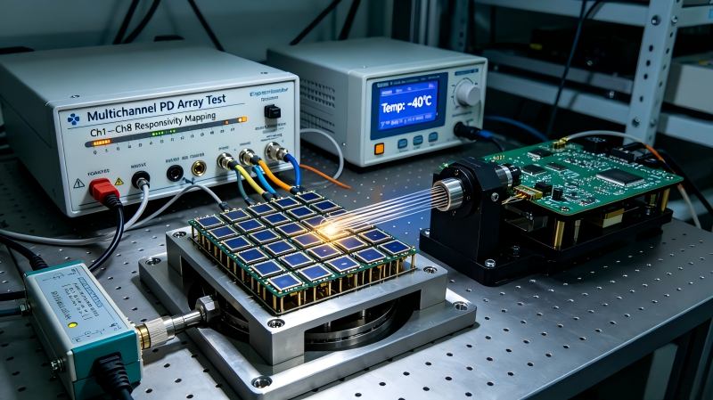
- Industrial & Field Deployments: Temperature swings from -40 °C to +85 °C cause severe dark current drift and sensitivity degradation. Thermo-Electric Coolers (TEC) are frequently integrated into high-sensitivity modules to stabilize performance.
Part 13: Saturation Power & Dynamic Range
System designers frequently focus exclusively on maximum sensitivity, neglecting the upper limit of detector operation: saturation power. When high optical power floods the detector, space-charge effects screen the internal electric field, causing gain compression, non-linearity, and phase distortion.
High-performance systems require a broad dynamic range—the operational window between the minimum detectable signal (sensitivity limit) and maximum input power before saturation. High sensitivity must be balanced against linear power handling.
Part 14: Practical Design Tips for Maximizing Sensitivity
When engineering high-sensitivity optical receiving systems, implement the following practical checklist:
- Match Wavelength: Select a photodiode optimized specifically for your optical source (e.g., InGaAs for 1310/1550 nm).
- Minimize Connector Loss: Use high-quality FC/APC or LC/APC connectors with precision alignment sleeves.
- Deploy a Low-Noise TIA: Pair the photodiode with a low-noise photodetector front-end amplifier stage.
- Shield Against EMI: Enclose sensitive photodiode-TIA front-ends in shielded metal packages to block RF interference.
- Optimize Bias Voltage: Set reverse bias at the sweet spot balancing full depletion speed against dark current rise.
- Maintain Clean Fiber End-Faces: Inspect and clean optical connectors before every mating cycle to prevent insertion loss.
- Implement Thermal Control: Integrate TEC cooling for applications requiring stable low-noise performance.
- Right-Size System Bandwidth: Do not select higher bandwidth than necessary; limit receiver bandwidth to control integrated thermal noise.
Part 15: How to Choose a High-Sensitivity High-Speed Photodetector
Selecting the optimal high speed photodetector sensitivity module requires matching specifications to application requirements:
1. Optical Communication (Datacom & Telecom)
- Key Requirements: High bandwidth (28 GHz, 40 GHz, 70 GHz), low noise floor, 1310 nm / 1550 nm wavelength operation.
- Recommendation: Integrated InGaAs PIN-TIA or Avalanche Photodiode (APD) modules featuring high responsivity and differential outputs.
2. RF Photonics & Microwave Links
- Key Requirements: Large dynamic range, high linearity, high RF output power capability, minimal phase noise.
- Recommendation: Highly linear Modified Uni-Traveling Carrier (MUTC) or waveguide InGaAs photodiodes handling high optical power without saturation.
3. LiDAR & Time-of-Flight (ToF) Sensing
- Key Requirements: Fast rise time, high pulse sensitivity, ultra-low timing jitter.
- Recommendation: High-gain InGaAs APDs or Silicon Photomultipliers (SiPM / SPAD arrays) for single-photon counting sensitivity.
4. Laboratory Measurement & R&D
- Key Requirements: Wide wavelength spectral response, flat frequency response, stable calibrated responsivity.
- Recommendation: Fiber-coupled or free-space broad-spectrum low-noise photodetectors with integrated DC-coupled low-noise amplifiers.
Frequently Asked Questions
1. What is the difference between sensitivity and responsivity?
Responsivity (A/W) measures how efficiently a photodetector converts input optical power into photocurrent, representing signal conversion gain. In contrast, sensitivity defines the minimum detectable optical power needed to achieve a required Signal-to-Noise Ratio (SNR) or Bit Error Rate (BER). Sensitivity accounts for both responsivity and internal/external noise current; a detector with high responsivity can still suffer from poor sensitivity if its dark current or amplifier noise floor is excessively high.
2. How does NEP affect photodetector sensitivity?
Noise Equivalent Power (NEP) represents the optical power that generates a photocurrent equal to the noise floor at a 1 Hz bandwidth. Because NEP quantifies the noise-limited detection threshold, a lower NEP corresponds directly to higher photodetector sensitivity. Lower NEP values indicate that the detector can resolve weaker optical signals above its intrinsic electronic noise.
3. Why does higher bandwidth reduce sensitivity?
Increasing operational bandwidth decreases sensitivity due to two primary factors: first, total integrated noise power grows linearly with bandwidth (in2 ∝ Δf), elevating the noise floor. Second, high-bandwidth designs require smaller transimpedance amplifier feedback resistors and reduced active areas to minimize RC time constants, which limits optical gain and optical collection efficiency.
4. What is the role of quantum efficiency?
Quantum Efficiency (QE) is the percentage of incident photons that successfully generate collected electron-hole pairs. High QE directly boosts photodetector responsivity, which proportionally increases the generated signal photocurrent relative to fixed internal noise, thereby directly improving overall photodetector sensitivity.
5. Which photodetector material offers the highest sensitivity at 1550 nm?
Indium Gallium Arsenide (InGaAs) provides the highest sensitivity at 1550 nm. Silicon is transparent at 1550 nm due to its wider bandgap, while Germanium exhibits significantly higher dark current and lower quantum efficiency. InGaAs features an ideal energy bandgap for C-band/L-band telecom, achieving high quantum efficiency (>85–90%) and ultra-low dark current.
6. How does temperature affect photodetector performance?
Temperature increases cause exponential growth in dark current (doubling every 8 °C to 10 °C, directly elevating shot noise and degrading minimum detectable sensitivity. Additionally, temperature changes cause semiconductor bandgap shifts, slightly altering the absorption edge and spectral responsivity. Thermal stabilization (e.g., using TEC cooling) is critical for low-noise applications.