What Are the Mechanisms of Photodetectors?
There are three common photoelectric conversions (conversion of absorbed photons into charges) mechanisms in photodetectors, which are the photoconductive effect (PCE), photovoltaic effect (PVE), and photo thermoelectric effect (PTE).
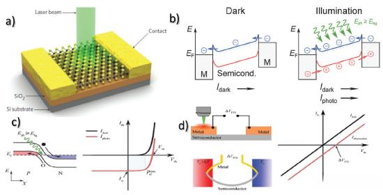
Fig. 1 (a) Schematic diagram of the structure of 2D photodetector based on SiO2/Si substrate. (b) Schematic diagram of the photoconductive effect: in a dark field and under the light. (c) Schematic diagram of the photovoltaic effect: band alignment in the PN junction and I–V curves under dark-field & light conditions. (d) Schematic diagram of the photo thermoelectric effect: the “hot circuit” of the field effect transistor device and the Ids-Vds characteristics under dark field & light.
Photoconductive Effect-PCE
This effect can be simply expressed as the material absorbing photons to enhance the conductivity of two-dimensional (2D) materials (Fig. 1b). Under a dark field when a voltage is applied to the device, the current between the two electrodes is very small. Under the light, the absorption of light by the material will generate electron-hole pairs with energy greater than the band gap, and the drift of electrons and holes in different directions forms a photocurrent, which increases the current between the electrodes and enhances the conductivity of the device, that is the photoconductive effect.
Photovoltaic effect-PVE
This effect can be simply expressed as the device absorbs photons under illumination to excite electron-hole pairs, which are separated by the internal electric field to generate a voltage, thereby forming a photocurrent. Some interfaces can establish internal electric fields, such as Schottky junctions or PN junctions (Fig. 1c). In the dark field, the device exhibits nonlinear I-V characteristics due to the existence of the PN junction, and the current increases exponentially with the voltage. When illuminated, the electron-hole pairs excited by absorbing photons can be separated by the built-in electric field without external voltage, leading to an increase in photocurrent. At this time, a reverse voltage bias is applied to the device, the photo-generated carriers move in the opposite direction, the reverse current increases and the photon energy is converted into electrical energy through the photovoltaic effect. This mechanism enables the photodetector to operate with extremely low power consumption.
Photothermoelectric effect – PTE
This effect can be simply expressed as the device generates a thermoelectric effect under illumination (Fig. 1d). When light energy is absorbed, the temperature of the heat-sensing element in the device increases, and this light-induced heating leads to the formation of a temperature gradient in the semiconductor. Due to the Seebeck effect [The Seebeck effect means that when there is a temperature gradient in an electronic conductor, an electromotive force difference will be generated at both ends of the conductor. This effect is exploited to generate electricity in thermoelectric devices such as thermal batteries and thermoelectric converters. In the thermoelectric effect, a temperature difference causes the thermal diffusion of electrons in a conductor, creating an electromotive force difference. The Seebeck effect was first discovered in 1821 by German physicist Thomas Seebeck. ], the temperature difference ΔT at both ends of the semiconductor channel can be converted into a voltage difference ΔV = SˑΔT, where ΔV has a linear relationship with ΔT.


