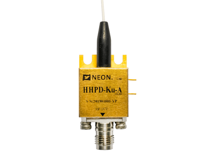
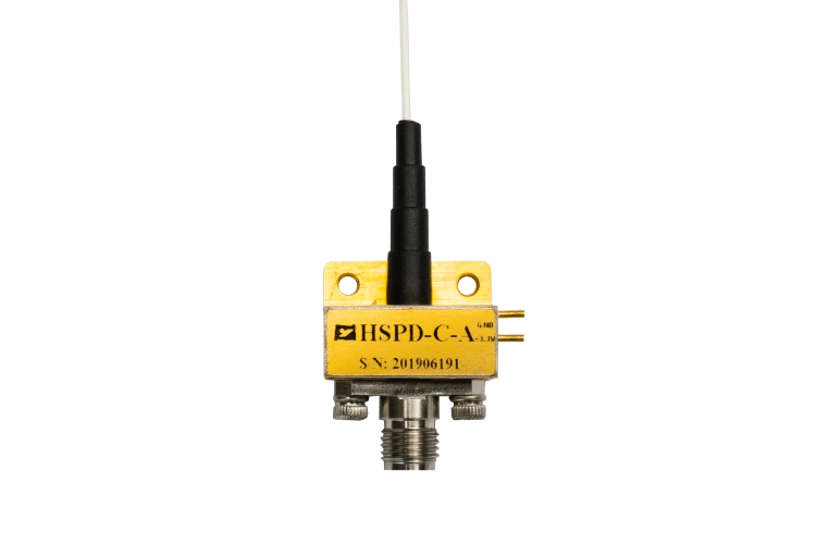
How does the High Speed Photodetector Work?
What is a High-Speed Photodetector?
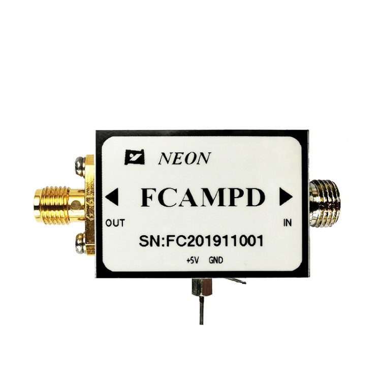
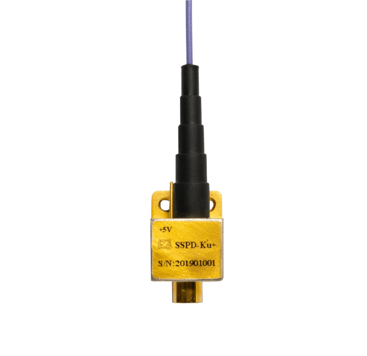
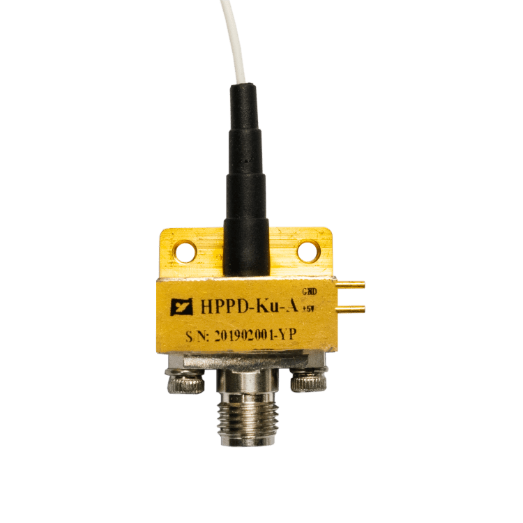
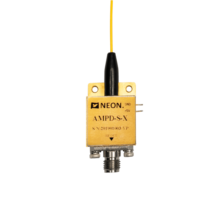
The photodetector realizes the role of converting light into electricity in the optical communication system. This is mainly based on the photovoltaic effect of semiconductor materials. The so-called photovoltaic effect refers to the uneven semiconductor or semiconductor and metal bonding between different parts of the light. The phenomenon of potential difference. With the continuous advancement of science and technology, there is now a newer technology high-speed photodetector.
The photoconductivity effect refers to the phenomenon that electrons absorb the photon energy from the bonded state to the free state under the action of light, which causes the conductivity of the material to change. That is when light is irradiated on the photoconductor if the photoconductor is based It is a kind of physics in that the electrons in the valence band of the photoelectric material will be excited to the conduction band to increase the conductivity of the photoconductor, which means that the conductivity of the irradiated material changes due to radiation. The phenomenon, photons act on the photoconductive material, forming intrinsic absorption or impurity absorption, and generating additional photo-generated carriers, which changes the conductivity of the semiconductor and produces a photoconductive effect.
The Working Principle of High-Speed Photodetector
The basic working mechanism of the photodetector includes three processes:
- Photo-generated carriers are generated under illumination;
- Carriers diffuse or drift to form currents;
- The photocurrent is amplified and converted into a voltage signal in the amplifying circuit.
When the detector surface is illuminated by light, if the material forbidden bandwidth is less than the energy of the incident photon, ie Eg<hv, the valence band electrons can transition to the conduction band to form a photocurrent.
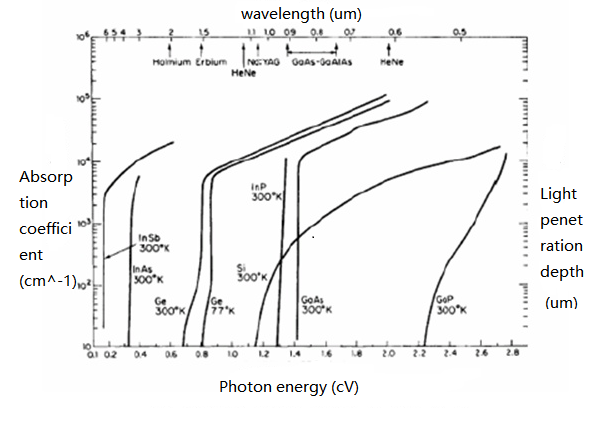
When light is transmitted in a semiconductor, the energy of the light wave will gradually attenuate as it propagates. The reason is that photons are absorbed in the semiconductor. The most important absorption of a photon by semiconductors is intrinsic absorption, which is divided into direct transition and indirect transition. By testing the intrinsic absorption spectrum of semiconductors, in addition to information such as the forbidden bandwidth of semiconductors, it can also be used to distinguish direct bandgap semiconductors and indirect bandgap semiconductors.
Intrinsic absorption causes the absorption coefficient of the material to be relatively high, and because of the energy band structure of the semiconductor, the semiconductor has a continuous absorption spectrum. It can be seen from the absorption spectrum that when the intrinsic absorption starts, the absorption spectrum of the semiconductor has an obvious absorption edge. But for silicon material, because it is an indirect bandgap material, it has a lower transition probability compared with the third and fifth group materials, so it has a very small absorption coefficient, and at the same time leads to the absorption of light in the silicon material under the irradiation of photons of the same energy. The depth is greater. The absorption edge of the direct bandgap material is much steeper than that of the indirect bandgap material. The figure shows the incident light wavelength, light absorption coefficient, and penetration of several commonly used semiconductor materials (such as GaAs, InP, InAs, Si, Ge, GaP, etc.) Deep relationship.
Performance Indicators of High-Speed Photodetectors
The performance indicators of photodetectors are mainly composed of indicators such as response speed and intrinsic bandwidth, photocurrent, dark current, and noise.
The response speed can be expressed by the transit time of photogenerated carriers. The external frequency response of the carrier transit time is the bandwidth of the detector. The transit time of photogenerated carriers is manifested in two parts in the change of photogenerated current: rise time and fall time. Usually, the larger of the rise time and the fall time is used to measure the response speed of the detector. The main factors that determine the response speed of the detector are:
⑴. Carrier transit time in the depletion zone: The carrier transit time is the most important factor affecting the response speed of the detector. When the electric field intensity in the depletion zone reaches the maximum, Wd represents the maximum drift speed of the carrier. W represents the width of the depletion region, then the carrier transit time is:
t=W/Vd
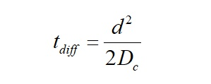
⑵ Carrier diffusion time outside the depletion zone: The speed of carrier diffusion is slow, and most of the carriers generated outside the depletion zone have a very short lifespan, and the recombination occurs quickly. Therefore, only the carriers close to the depletion region can reach the depletion region through diffusion motion and drift in the electric field to generate photocurrent. Dc represents the diffusion coefficient of carriers, d represents the diffusion distance, and the diffusion time is as follows:
⑶ Depletion area capacitance of the photodiode: the larger the capacitance, the slower the response speed.
To achieve the best response speed of the detector, it is necessary to compromise between the thickness of the absorption layer of the detector and the area of the photodetector. For example, increasing the thickness of the absorption layer of the detector material can effectively reduce the plate capacitance of the depletion region, and at the same time, increasing the thickness of the absorption layer can improve the quantum efficiency of the detector. However, the increase in the thickness of the absorption layer causes the width of the depletion region to become larger, which may reduce the response speed of the detector due to the longer transit time of the photo-generated carriers.
⑷Dark current and noise
Photocurrent refers to the photogenerated current generated by the photodetector under the illumination of incident light. Dark current can be defined as the leakage current of the detector when there is no light incident. Its size affects the sensitivity of the optical receiver and is one of the main indicators of the detector. Dark current mainly includes the following:
①The minority carrier diffusion current at the boundary of the depletion zone;
②Carrier generation-recombination current, which can effectively reduce the generation of carriers by eliminating the lattice defects of silicon materials during processing. -Composite current, usually generated for high-purity single-crystal silicon-Composite current can be reduced to 2*1011A/nm2 or less;
③Surface leakage current, at the end of the manufacturing process, passivation treatment on the surface of the chip can reduce the surface leakage current Reduce to the order of 1011A/nm2.
Of course, the dark current is also affected by the detector’s operating temperature and bias voltage. The dark current and noise of the detector are inseparable. Usually, the noise of the photodetector is mainly divided into dark current noise, shot noise, and thermal noise:
- Dark current noise: For a photodetector, the minimum receivable optical power is determined by the dark current of the detector, so reducing the dark current of the detector can improve the sensitivity of the optical receiver;
- Shot noise: When the detector receives incident light, the shot noise is produced by the production of photons -In the process of compounding. Since the number of photo-generated carriers is subject to the Poisson statistical division, there is shot noise in the process of photo-generated carriers;
- Thermal noise: Since the random movement of electrons in the conductor will produce fluctuations in the voltage across the conductor, Thermal noise will be generated. The resistance contained in the circuit model of the photodetector is the main source of thermal noise.


